As the AI chip race intensifies, the technology used to stack and connect chips has become as strategically important as the chips themselves. That reality was underlined on Tuesday, when the world's largest chip equipment maker moved to double its stake in a Dutch specialist.
Applied Materials plans to raise its stake in BE Semiconductor Industries (BESI), a maker of advanced packaging equipment based in Duiven, Netherlands, from 9% to about 20%, according to Reuters reports cited by TrendForce on October 27. The purchase will be made under an accelerated share purchase agreement and is subject to US antitrust review.
BESI shares rose 8.5% in European trading on Tuesday, according to Reuters.
Limits on the stake
Applied Materials said it will not go above roughly 20% and does not seek a seat on BESI's board. The purchase price and total value were not disclosed.
Applied became BESI's largest shareholder when it acquired its 9% stake in April 2025. At the time, it described the investment as strategic and long-term, and said it had no plans to increase it. The decision to double the stake signals how important the partnership has become.
What hybrid bonding is
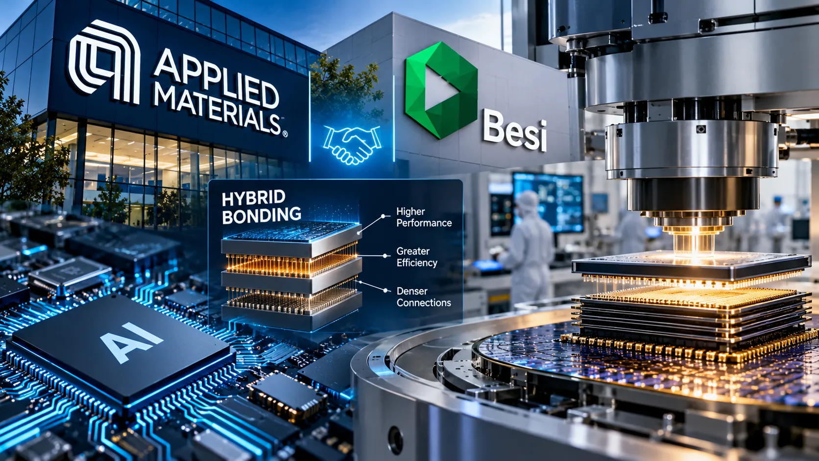
Hybrid bonding is an advanced technique for connecting chips by creating direct copper-to-copper links between them, without the tiny solder bumps used in traditional packaging. It allows much denser connections and shorter wiring between chips, improving performance and energy efficiency.
The technology is becoming critical for AI chips, which increasingly combine multiple smaller chips, or chiplets, in a single package, and for high-bandwidth memory, which stacks memory chips vertically. As AI processors grow more complex, the ability to connect chips efficiently becomes a key determinant of performance.
Applied Materials and BESI have collaborated on hybrid bonding since 2020 and jointly developed Kinex, a die-to-wafer hybrid bonding system.
BESI's surge in orders
Demand for BESI's equipment has surged. The company's third-quarter orders rose 96% year on year to €342.6 million, according to Reuters. Hybrid bonding orders in the first nine months of 2026 have already more than doubled the full-year 2025 level.
BESI reported 23 hybrid bonding customers and more than 215 cumulative systems shipped, according to its latest earnings release. The company is estimated to hold about 70% of the global market for hybrid bonding equipment.
Why Applied wants more
For Applied Materials, a larger stake in BESI strengthens its position in one of the fastest-growing segments of the semiconductor equipment market. Applied supplies a wide range of tools for chip manufacturing, from deposition and etching to inspection. Advanced packaging, once a less glamorous part of the industry, is now central to the AI chip roadmap.
By deepening its relationship with BESI, Applied can offer customers a more complete solution for advanced packaging, combining its own process technology with BESI's bonding equipment.
Antitrust scrutiny
The deal requires US antitrust review, reflecting regulators' scrutiny of consolidation in the semiconductor industry. Applied's commitment not to exceed about 20% and not to seek a board seat may be intended to address competition concerns.
Semiconductor equipment is a highly concentrated industry, with a small number of companies dominating key segments. Governments in the United States, Europe and Asia view the industry as strategically important and closely watch deals that could affect competition or supply chains.