TechFuture Tech2 MIN READ

ASML Plans Larger High-NA EUV Masks With TSMC, Intel and Samsung Support

ASML is working with TSMC, Intel Foundry and Samsung to move High-NA EUV lithography from 6-inch to 12-inch photomasks, a shift expected to lift system productivity by roughly 40% for next-generation AI chips.

By Shaym Kumar · Author9 September 2026
ASML Plans Larger High-NA EUV Masks With TSMC, Intel and Samsung Support

ASML announced on September 8, 2026, that it is working with major semiconductor manufacturers, including TSMC, Intel Foundry and Samsung Electronics, on a significant change to its most advanced High-NA extreme ultraviolet lithography systems, aimed at removing a practical constraint on the size of chips the machines can produce. The Dutch equipment maker plans to develop larger photomasks — moving from the industry's long-standing 6-inch standard to 12-inch masks — that could eventually enable production of substantially larger AI and data-centre processors.

Today's most advanced EUV systems can expose chips approaching 800 square millimetres, a limit that matters increasingly as AI accelerators from companies such as Nvidia and Google grow larger and more complex. High-NA EUV technology offers finer resolution than previous-generation lithography, but its smaller exposure field has complicated efforts to manufacture the largest data-centre chips without resorting to complex die-stitching techniques. ASML's proposed larger-mask approach is designed to let manufacturers capture High-NA's resolution advantages without forcing chip designers to shrink their most demanding processor designs.

The company said it expects the change to improve system productivity by approximately 40%, though full high-volume deployment of the larger-mask approach remains years away given the engineering complexity involved in redesigning both the lithography systems and the broader photomask supply chain that supports them. Intel has already begun accumulating substantial production experience with High-NA equipment, having recently passed one million processed 300-millimetre wafers using the technology — a milestone reached less than two and a half years after installing its first High-NA machine.
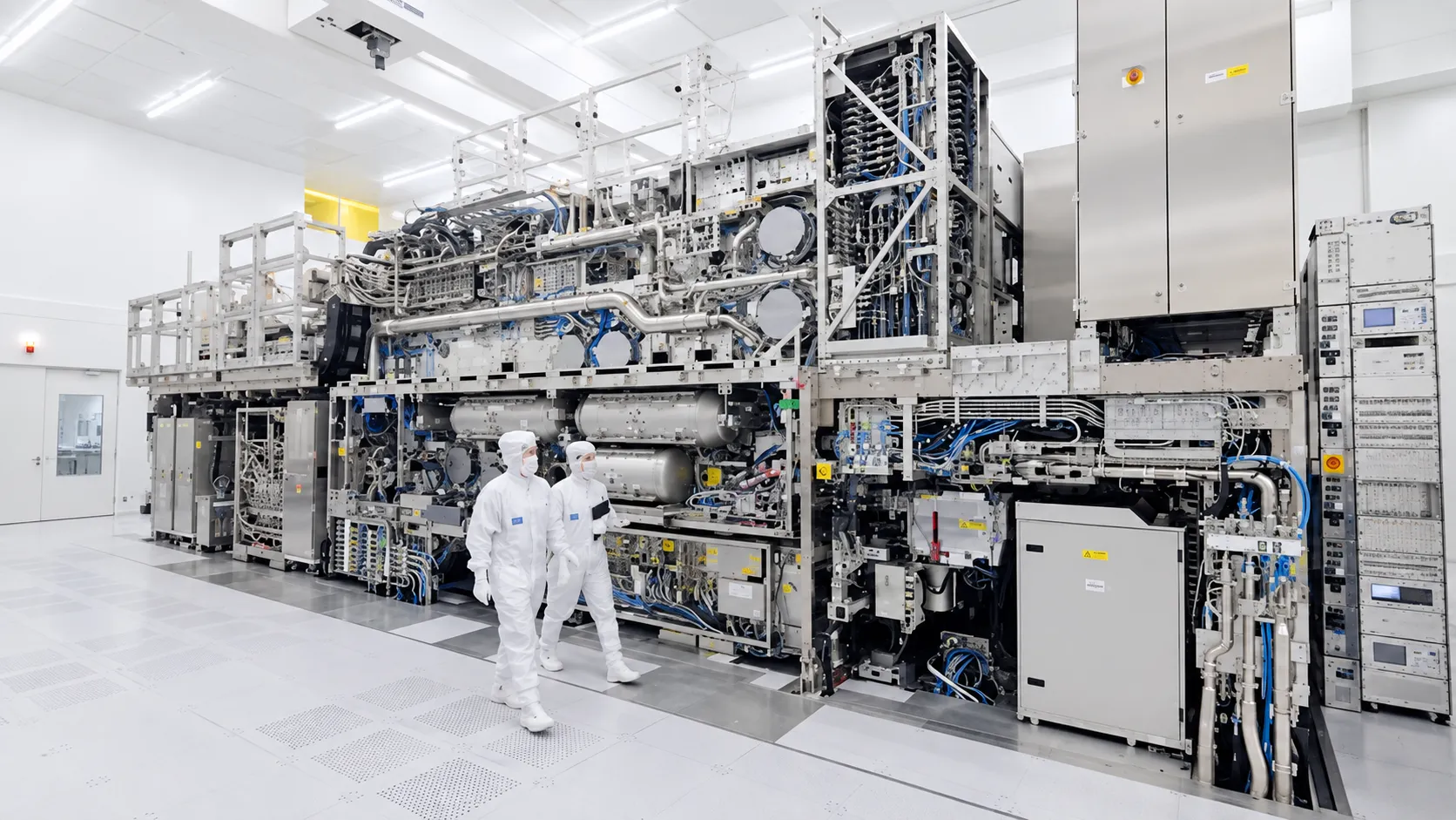
Removing the mask-size constraint could unlock a new generation of larger, more powerful AI processors that today's lithography systems simply cannot accommodate.
TIGI Technology Desk
ChatGPT Image Sep 9, 2026, 12_13_34 PM.png

The joint effort among ASML, TSMC, Intel Foundry and Samsung reflects the increasingly collaborative nature of leading-edge semiconductor manufacturing, where the capital intensity and technical complexity of next-generation lithography have made it impractical for any single company to advance the technology in isolation. As AI accelerators continue to grow larger, more complex and increasingly dependent on advanced packaging techniques, lithography constraints that were once considered obscure manufacturing details have become strategic bottlenecks shaping the architecture of future chip designs.

For the broader AI infrastructure buildout, resolving the mask-size constraint could have significant downstream effects. Chip designers currently must work within the physical limits imposed by existing lithography systems when architecting new AI accelerators, sometimes requiring compromises in performance or efficiency to accommodate manufacturing constraints. Larger masks would give designers considerably more flexibility, potentially enabling a new generation of larger, more powerful single-die processors optimised specifically for AI training and inference workloads.

Industry analysts note that the transition, while strategically important, will unfold gradually given the multi-year qualification cycles typical of advanced semiconductor manufacturing technology. Nonetheless, ASML's announcement signals that the industry's leading equipment maker and its most important customers are already planning several technology generations ahead, underscoring how central lithography roadmaps have become to the broader trajectory of AI hardware development globally.

TagsASMLSemiconductorsEUV LithographyTSMCIntelSamsungChip Manufacturing

Reader reviews

Sign in to rate and review this article.
Loading reviews…