Ayar Labs, the optical-interconnect startup developing technology to move data between AI chips using light rather than conventional electrical signalling, has secured an additional $150 million, bringing its total primary funding raised in 2026 to approximately $650 million. The round, confirmed on September 11, comes as the company prepares its co-packaged optical technology for high-volume production and simultaneously establishes a new design centre in Bengaluru, India.
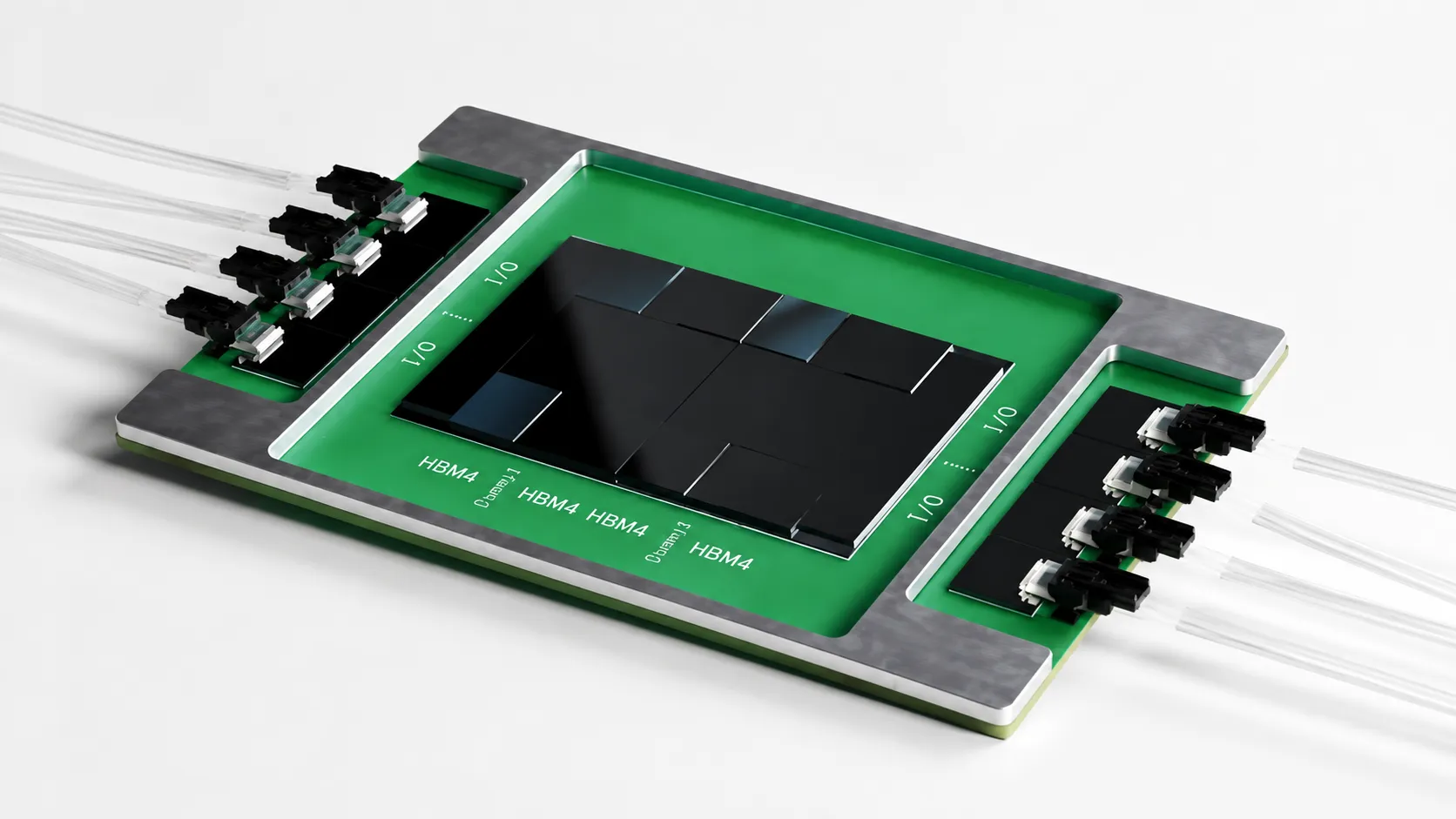
The company's core technology addresses a problem that has become increasingly urgent as AI infrastructure scales: moving enormous volumes of data between chips fast enough, and with low enough energy consumption, to keep pace with the growth in AI model size and the number of accelerators required to train and run them. As AI systems increasingly consist of thousands, and eventually potentially millions, of accelerators working in concert, the electrical interconnects traditionally used to link chips together are approaching physical limits in both bandwidth and power efficiency. Ayar Labs' co-packaged optics approach replaces at least part of that electrical signalling with light, which can carry more data with less energy loss over the distances relevant inside and between server racks.
Ayar's investor base already includes some of the most significant names in global semiconductors, with Nvidia, AMD, Intel, MediaTek and Alchip counted among its strategic investors and partners — an unusually broad coalition given that several of these companies compete directly with one another in other parts of the chip market. That breadth reflects the extent to which optical interconnect technology is increasingly viewed as foundational, horizontal infrastructure that benefits the entire AI hardware ecosystem rather than favouring any single chip vendor, making it a rare area where rival semiconductor giants have aligned around backing the same infrastructure supplier.
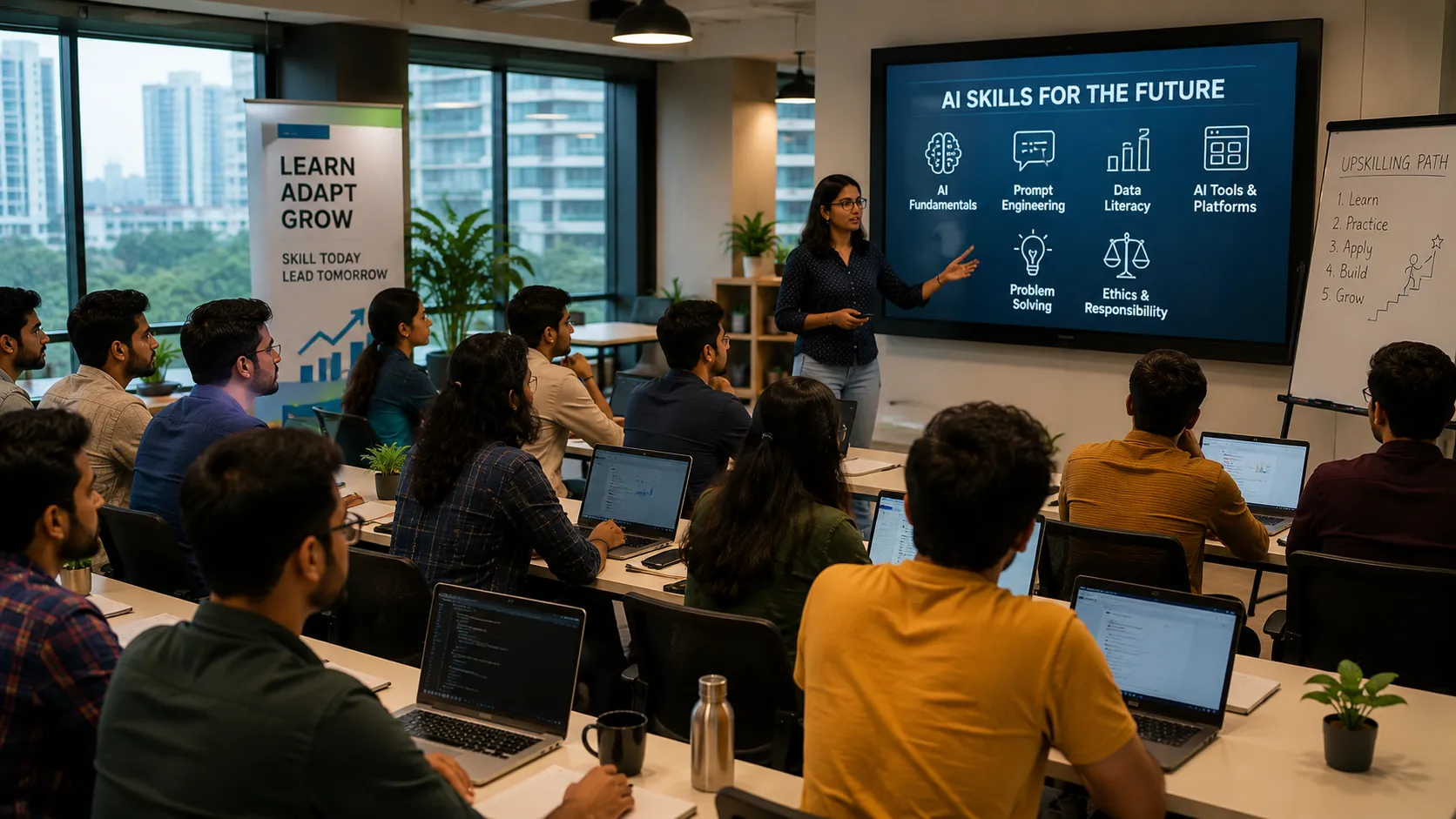
The decision to establish a design centre in Bengaluru is significant for India's growing role in the global semiconductor value chain. While India has for years supplied chip design and verification talent to global semiconductor companies through the engineering centres of firms such as Intel, Qualcomm and Texas Instruments, the establishment of a dedicated design centre by a well-funded, strategically positioned optical-interconnect startup signals continued confidence in India's chip-design talent pool specifically for cutting-edge, physically demanding photonics and packaging engineering — a more specialised discipline than conventional digital chip design.
The timing of Ayar Labs' raise and expansion coincides with an extraordinary period of capital deployment across AI infrastructure globally. Cloud and hyperscale companies have announced multi-gigawatt data-centre build-outs in recent days, alongside enormous cloud backlog figures and financing discussions involving government-backed loans to support data-centre supply chains — context that underscores just how much physical infrastructure, beyond the AI models themselves, is required to sustain the current pace of AI development. Interconnect technology sits at a critical chokepoint within that infrastructure build-out, since even the most capable AI accelerator chips are only as effective as the speed at which they can exchange data with one another.
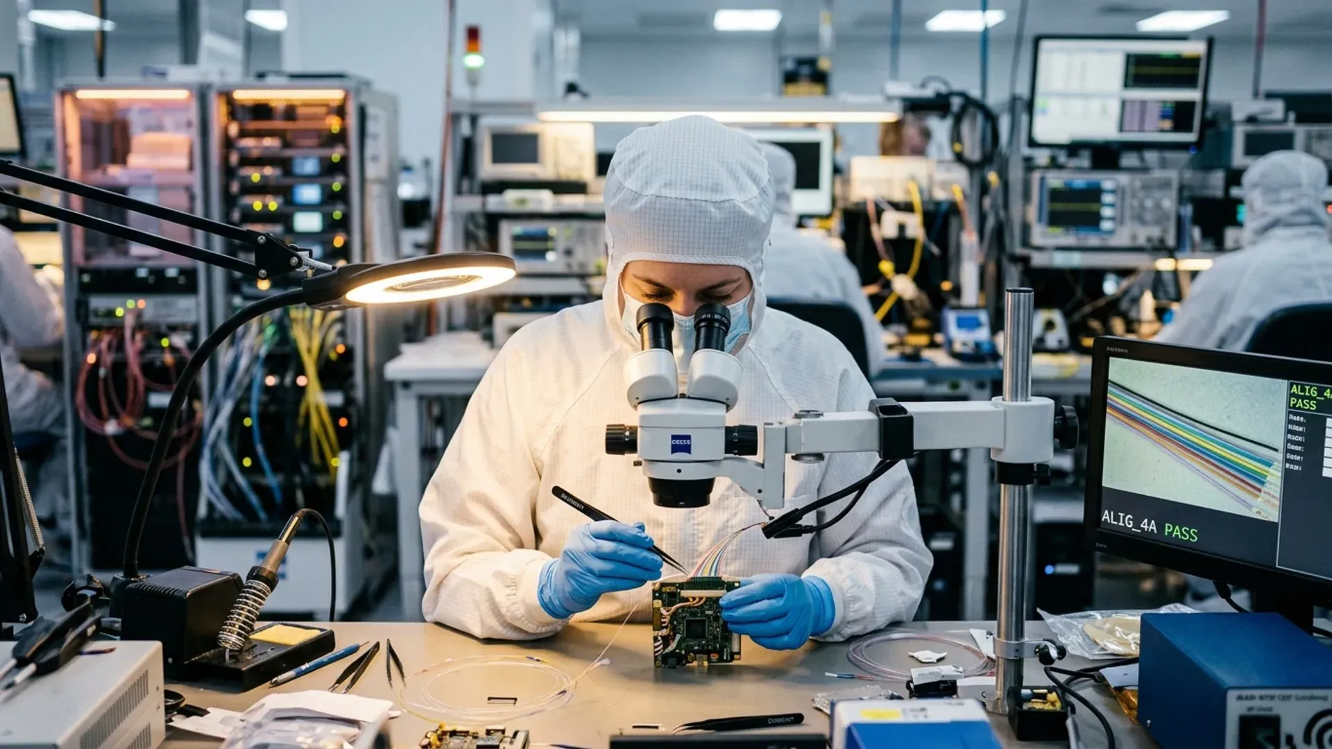
For Ayar Labs specifically, the challenge ahead lies less in securing capital — a task the company has clearly managed successfully throughout 2026 — than in proving it can move from strategic partnerships and pilot deployments to genuine high-volume production at costs competitive with, or justified relative to, traditional electrical interconnects. Photonics-based technologies have historically faced a difficult transition from laboratory-grade demonstrations to mass-manufacturable products, given the precision required in aligning optical components at the chip-packaging level.
The company has not disclosed the specific valuation attached to the latest $150 million tranche, nor detailed the scale of its planned Bengaluru operations in terms of headcount or investment commitment. Given the scale of Ayar's 2026 fundraising and the calibre of its strategic investor base, however, the Bengaluru centre is likely to be watched closely both as a marker of India's expanding role in frontier semiconductor engineering and as a signal of how central optical interconnects are becoming to the broader AI infrastructure build-out underway across the industry.