Morphotonics, a Netherlands-based deep-technology company specialising in large-area nanoimprint lithography, has raised €40 million to expand its manufacturing technology from augmented-reality displays into optical components for artificial-intelligence data centres.
The round, reported on 22 September 2026, drew a broad group of investors, including 3M Ventures, Innovation Industries, the regional development agency BOM, Invest-NL, the European Innovation Council Fund, the European Investment Bank and the family office Ernij Next.
A decade of building a manufacturing platform
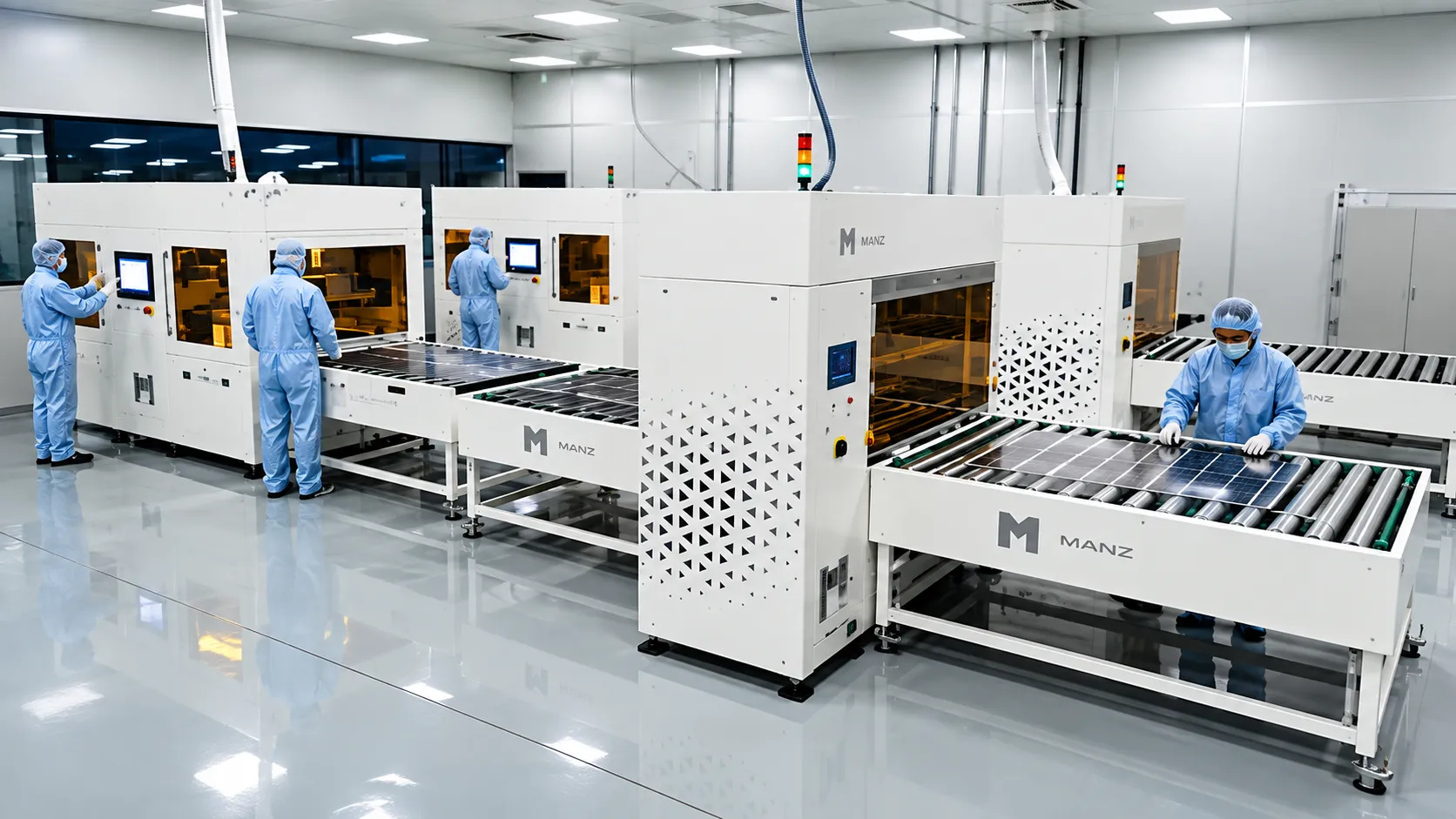
Morphotonics has spent more than a decade developing manufacturing systems that imprint extremely small optical structures onto materials at commercial scale. Nanoimprint lithography works by pressing a patterned mould into a resin layer on a substrate, replicating nanoscale features that can control how light travels through a material.
Compared with conventional lithography techniques used in semiconductor manufacturing, nanoimprint can be significantly cheaper for certain applications, particularly when patterns must be replicated over larger areas. The difficulty lies in achieving the precision, uniformity and yield required for high-volume production. Morphotonics' expertise is in making that process industrial.
From smart glasses to data centres
The company is best known for technology used to produce waveguides, the optical components that guide images into a wearer's field of view in augmented-reality glasses. Waveguides are among the most critical and costly components in AR devices, and their manufacturing has been a significant barrier to producing lightweight, affordable smart glasses at scale.
Morphotonics' next machine is expected to produce more than six million waveguides annually, a volume that points to the company's ambition to support mass-market AR devices as major technology companies invest in smart glasses.
The potentially larger long-term opportunity, however, may be in data centres. Morphotonics is moving into co-packaged optics, an emerging approach in which optical components are integrated closely with processors and switches, allowing data to be transmitted using light rather than conventional electrical connections over longer distances within a system.
Why light matters for AI
The rise of large AI models has transformed data-centre design. Training and running these models requires thousands of accelerators working together, exchanging enormous volumes of data. As clusters grow, the connections between chips have become one of the biggest constraints on performance and energy efficiency.
Electrical connections consume more power and lose signal quality as data rates rise and distances increase. Optical interconnects can carry more data over longer distances with lower energy consumption per bit. Co-packaged optics takes that advantage further by placing optical engines directly alongside switch or processor chips, reducing the power-hungry electrical paths between them.
Major semiconductor and networking companies have been developing co-packaged optics for several years, and the technology is expected to play a growing role in next-generation AI infrastructure. That creates demand for manufacturing techniques capable of producing precise optical structures at scale and at acceptable cost, the capability Morphotonics has spent years building.
A European deep-tech statement
The investor syndicate reflects strong institutional support for European deep technology. The European Innovation Council Fund and the European Investment Bank have become important backers of strategic technologies in Europe, while Invest-NL and BOM represent Dutch public support for industrial innovation. 3M Ventures brings a strategic dimension from one of the world's leading materials-science companies, and Innovation Industries is a Dutch investor focused on deep tech.